![]()

![]()
SOP ASSEMBLY PHOTO TOUR
Shown below are over 60 links to photos, with corresponding narrative, providing a step-by-step overview of the SOP printed circuit card assembly operation. Oscilloscope waveforms of signals at various points in the working SOP board, and typical RF probe voltage measurements, are provided to help builders have the confidence that their boards are being assembled correctly.
This Photo Tour is intended to be used in conjunction with the exhaustive text narrative provided in the SOP Manual, so we won't be duplicating explanations or providing too much redundant information.
Enjoy! And please be sure to ask questions if anything is unclear along the way. There's a growing number of QRPers who are getting their SOP Receivers working ... the excitement is building!
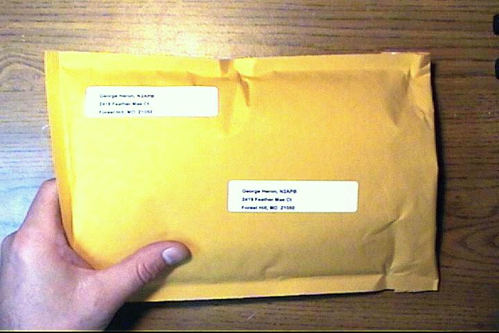
Photo 1: Mailing package -- This is what it looks like when it arrives in your mailbox. Even includes all options if you ordered them. (Of course, yours will hopefully have a cancelled stamp in the corner!)
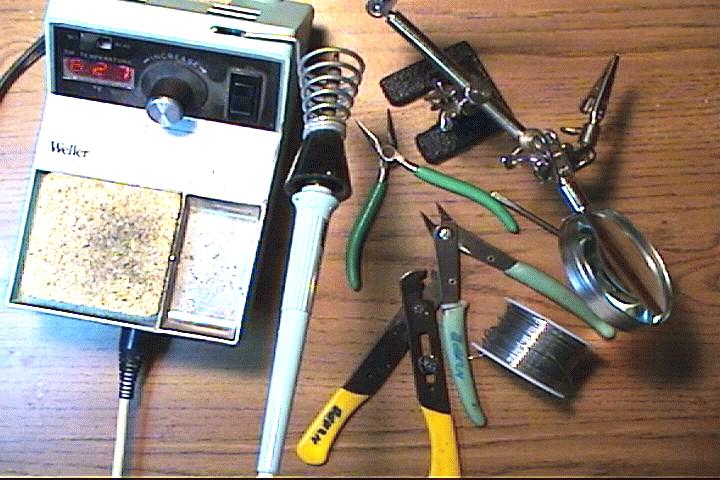
Photo 2: Tools to have handy -- Here are some of the tools I find pretty useful in assembling such a kit as the SOP: temperature-controlled soldering station (660-degrees F is the setting I use most often), wire strippers, needle nose pliers, side cutters, 60/40 rosin core solder and a circuit board holder with magnifying lens (which is real handy in identifying those small component values)
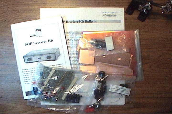
Photo 3: Open up the mailing package to see what's inside -- The basic kit contains the SOP Manual booklet, a Bulletin letter with Errata Sheets and updated schematic & layout diagrams, and a sealed plastic bag on the left containing the board-mounted components and pcb. Other options can be seen in this photo in their separate sealed plastic bags: Homebrew Enclosure (upper right), Hardware Controls (to the right of the basic kit bag), and the AFA (next on the right).
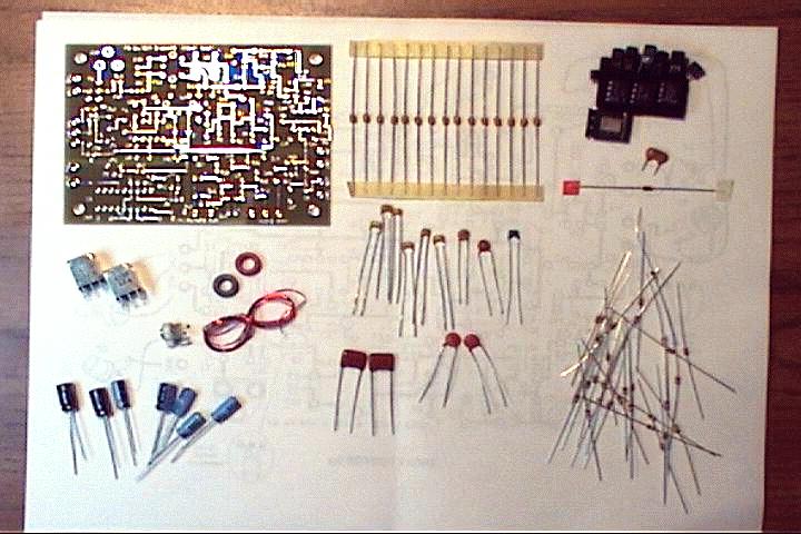
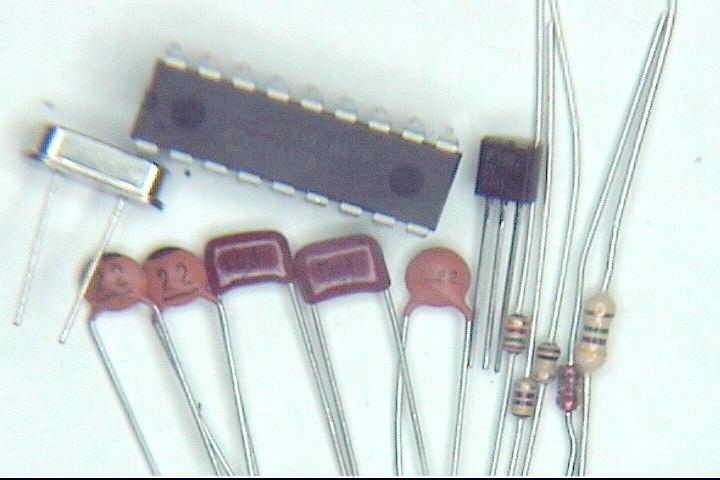
Photo 4: All the basic kit parts arranged on the table -- The first thing you should do is a careful inventory, comparing parts to the latest Part List to ensure that you have everything before you get started. Laying out the parts as shown in this photo makes it easier to locate a component when going down the Parts List.
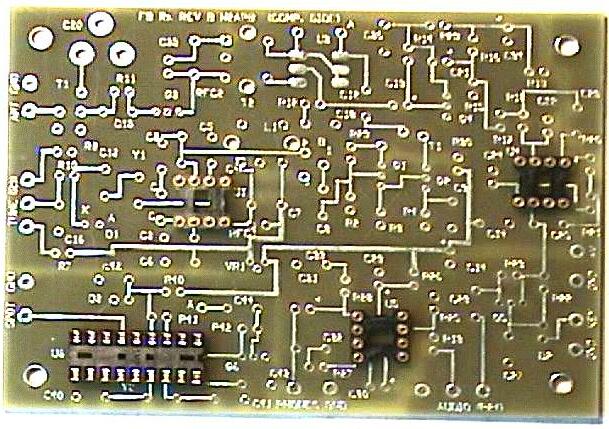
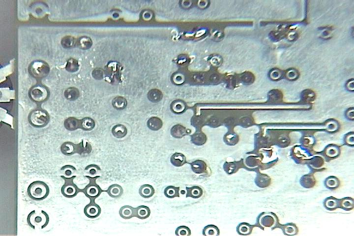
Photo 5: An almost-bare printed circuit board -- Here's a shot of the pc board with nothing but sockets installed on it. Note that IC sockets are not included in the kit, but you may find it advantageous to use them if you plan on doing some experimenting later on with this project. Additionally, the use of sockets makes it a breeze to debug your project if there are problems getting it working.
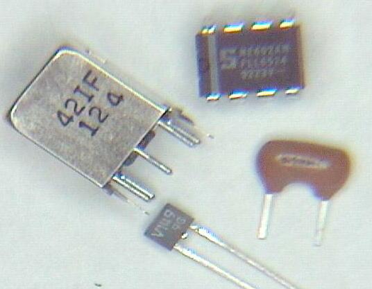
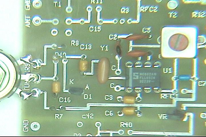
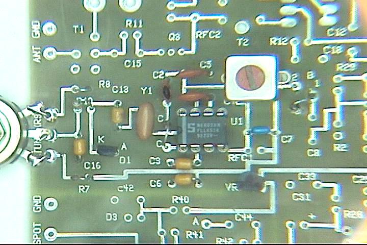
Photo 6: The first set of components for the Local Oscillator -- Here are the components used in the first assembly step of the manual: U1, L1, D1 and Y1. Note the unusual shape of the ceramic resonator Y1, and the 2-leaded varicap diode D1.
Photo 7: We use lots of 0.1uF bypass capacitors in this kit
Photo 8: The capacitors used in the LO -- Pictured here are C13, C16, C2, C3, C4, C5, C6, and C7.
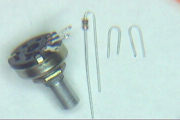
Photo 9: The resistors controlling the voltage to the varicap -- Here's a shot of the 10K potentiometer (from your junkbox or from the Controls Option), the mysterious missing 100K R10, and the jumpers used for now as the "padding resistors".
Photo 10: All LO components in place on the board -- This is what the LO should look like all together. Notice that I didn't put the jumper from pad C to pad C for this photo, although it is indeed needed for 40m operation. Also notice that this is the first time I show my technique for connecting external components to the board ... for simplicity during assembly and test, I connect the potentiometers, jacks, switches, etc right on the edge of the board. Once the board is tested and working, I disconnect these external components and locate the board in its enclosure with the controls and jacks in the front/rear panels.
Photo 11: Bottom side of the LO portion of the board -- Nothing special here other than showing the careful soldering and subsequent close inspection of every pad soldered on the bottom of the board. As experienced as I am, I still had a bunch of small solder shorts that I caught during this inspection process. (In order to make soldering more foolproof, we will be making the pads, traces and spacing-to-ground all bigger in the next iteration of the pc board.)
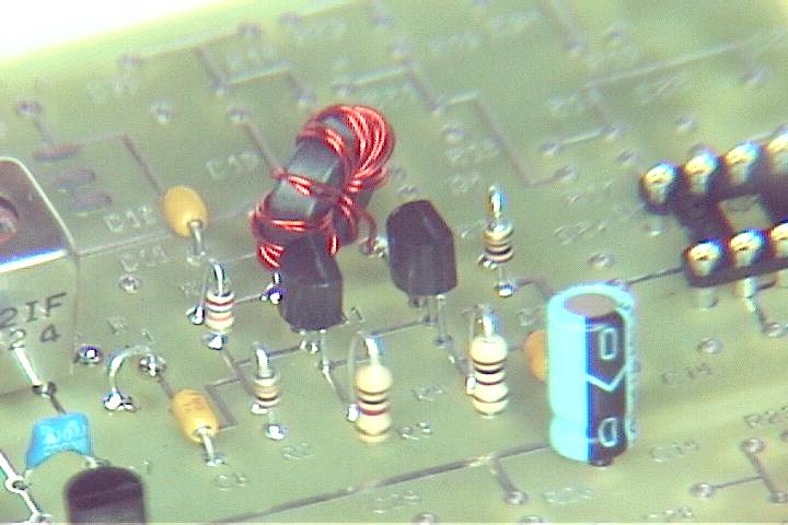
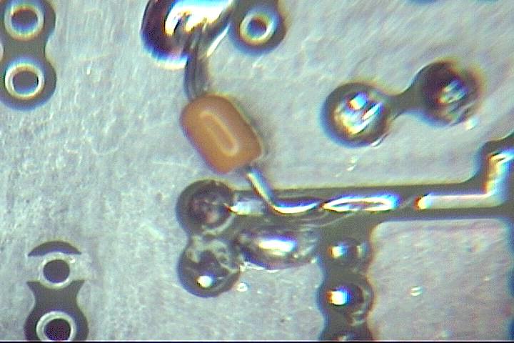
Photo 12: Close-up of L2 IF can on board -- Note that the IF can is positioned approx 1/16" up off the board. Mounting it in this manner will ensure that the outside can doesn't short against the trace on the top of the board. (A solder mask on the next rev of the board will help reduce the potential for this kind of a problem from happening.)
Photo 13: All LO components in place now -- Including that C-C jumper mentioned in Photo 10. Also in place is the B1-B3 jumper (just to the right of the L1 can) that passes the 40m signal on to the LO Buffer stage.
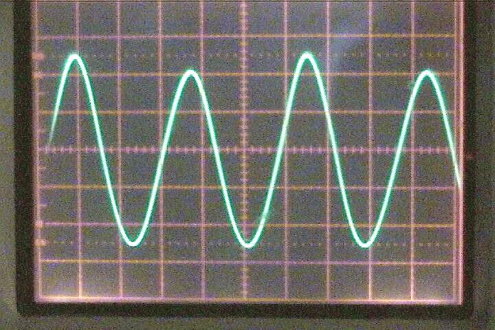
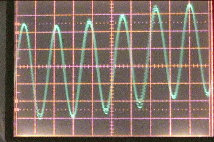
Photo 14: Apply power and ... LO Waveform! -- Here's a shot of an oscilloscope trace taken at the output of the LO (at the B jumper). The scope settings are .2V/div (V) and 0.5us/div (H), so we have about a 1V peak-to-peak (1Vpp) here. The reading you'd get on an RF probe of the type shown at the back of the Manual would be about half of that. I got a 5.86V reading on mine. Note that I used a 9V battery as the power source, but that doesn't matter here because the LO is supplied power by the 6V regulator VR1. My VR1 output was 5.86 volts DC.
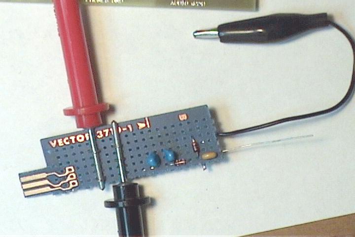
Photo 15: RF Probe construction -- Speaking of the RF probe, I thought I'd show the quick breadboard I made for mine. It's just a piece of scrap perf board with the two diodes and two caps stuck in. I kept one of the leads of the end cap sticking out as my "probe", and used half of an old clip lead as my (short) ground clip. if you look carefully, you'll see that I fashioned some scrap wire leads as little clips to hold my VOM probes in place.
Photo 16: Close-up of the VOM probe retaining wires -- I just slide the VOM probe into both of these home-made clips and it's held nicely in place.
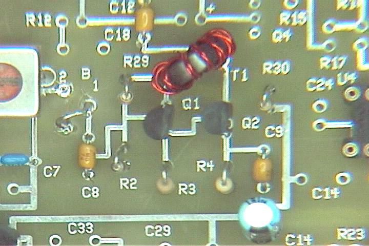
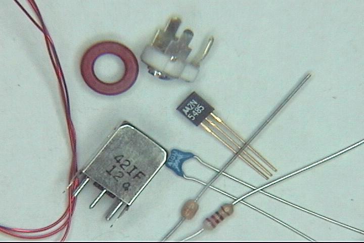
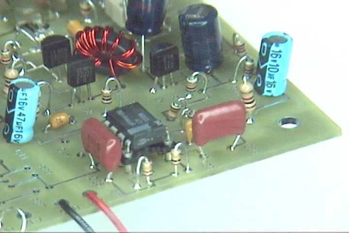
Photo 17: Components for the LO Buffer -- Here you see Q1, Q2, R2, R3, R4, R30, C8, C9, C10, C12, C37, the toroid core and the magnet wire. By the way, note the polarity of the electrolytic capacitor C37 ... it's negative lead is indicated with the thick black bar (with "-" embedded in it) shown here.
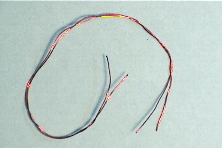
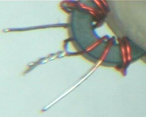
Photo 18: The twisted magnet wires make it "bifilar" -- Here's a shot of the two 7" lengths of magnet wire loosely twisted together by hand.
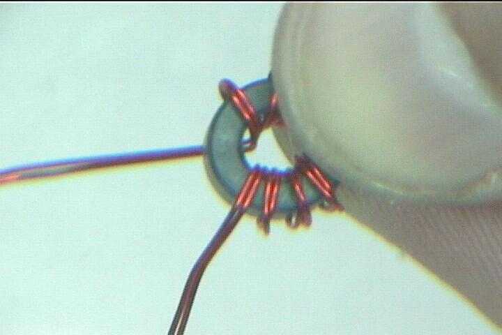
Photo 19: Toroid T1 with 10 bifilar windings -- This is how it should look after putting 10 turns of the twisted wire through the black FT37-43 toroid core.
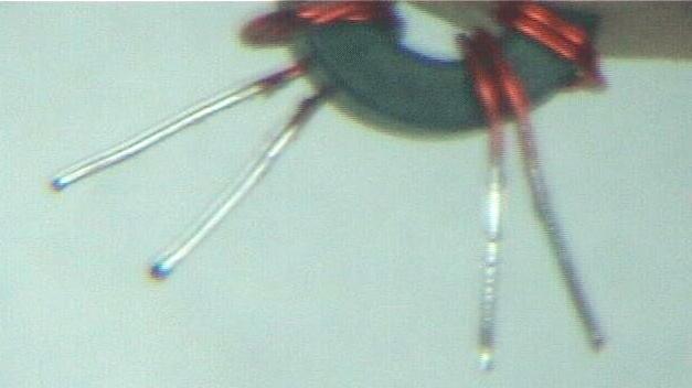
Photo 20: T1 leads are trimmed and tinned -- Here I've trimmed the leads to about 1/2" and stripped the enamel coating off the ends using the "heated soldering iron" technique described in the text. Most guys don't believe this technique works, but it really does!
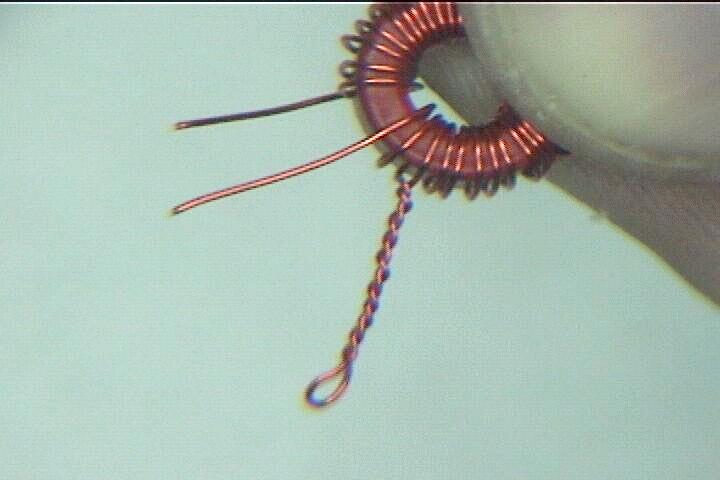
Photo 21: Creating the T1 center tap -- After identifying two different wires on either end of the winding, I twisted them tightly together to form the center tap of the transformer.
Photo 22: LO Buffer components installed on the board -- Notice the 45-degree angle that T1 is at ... let it take on its own positioning on the board, and don't force it to be rectilinear, or in-line with the other components.
Photo 23: LO Buffer components, side view -- Here's a side view of the LO Buffer components to better show the transformer and resistor mountings.
Photo 24: LO side view -- Looking back to the LO again, but this timee with a side view, you can see the component mountings better. Also notice another trick I use in construction with sensitive, or otherwise replaceable components. I used little machined pins (off a sacrificed IC socket) in which are mounted the varicap diode and ceramic resonator. This gives me an easy way to swap in different frequency-determining components ... this is useful in characterizing the board, so perhaps most builders would not need or want to be doing this. Just an idea to keep in your bag of tricks.
Photo 25: Underside mounting of C10 -- As the text and picture in the Manual shows, you need to solder C10 to the bottom of the board. Here's how mine looks.
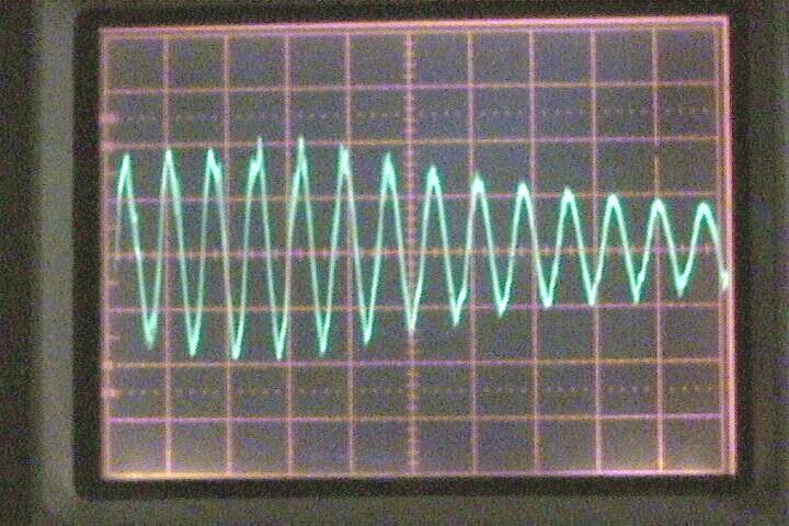
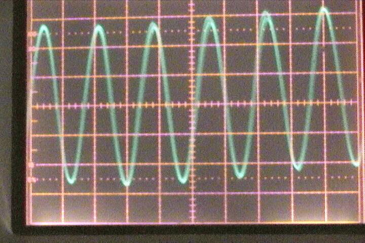
Photo 26: Scope waveform of LO Buffer output -- Here's the crazy signal shown at the output of the LO Buffer (on top end of C12). Scope settings: 10V/div and .2us/div, so we have our 7MHz signal again, with about a 28Vpp asymmetrical signal. Again, I was using a 9V battery as the power source at this point, and this truly has a bearing on the voltage seen at this point. Note that the buffer is unterminated (i.e., there's no load on it yet, so the waveform looks quite ragged and quite larger than one would expect.) My RF probe reads about 13.94V at this point. Note that this signal drops down to about 1.5Vpp when the mixer is soldered in place, and the signal becomes much cleaner and much more periodic. So don;t worry about seeing the ratty signal at this stage of assembly!
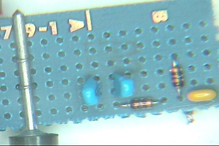
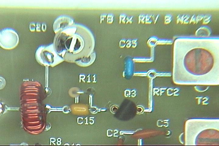
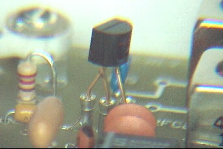
Photo 28: RF Pre-Amp Components -- Here's a shot of the components used in the RF Pre-Amp circuit; C20, C15, R11, Q3, T2 can, T3 core and magnet wire, and the mysterious C35 100pF capacitor that wasn't mentioned in the text.
Photo 29: T3 wound with the magnet wire -- This view of T3 almost complete is shown wound with #28 wire. Builders found that the #26 wire supplied in the kit was too thick to get 36 turns around the core, so an additional length of #28 wire was sent to all first round customers. Note the twisted loop after putting two turns through the core. This will become the secondary tap.
Photo 30: T3 primary added and leads are tinned -- Here I've added a two-turn primary wire, snipped all leads of to a short length, and tinned them as described before. Note that the proper orientation of the primary and secondary leads at this point will make insertion of the toroid onto the board much easier.
Photo 31: RF Pre-Amp components in place on the board -- Note the proper orientation of trimmer cap C20. Also note the slight twisted orientation of Q3 to accommodate the swapping of two of the leads in the pads. (See next photo.)
Photo 32: Side view of Q3 -- Shows the swapping of two leads, as illustrated by the diagram in the revised Parts Layout (dated 6/20/00, or later)
Photo 33: Side view of T1 in place -- Note the primary connections. And as with all toroid windings ... be very careful to tin the leads far enough up close to the core. If care is not exercised, poorly-stripped enamel will inhibit a good solder connection.
Photo 34: Jumper the LO signal over to the RF front end -- For testing purposes, we want to temporarily jumper the output of the LO Buffer (C12) over to the ANT input of the RF Pre-Amp. This will provide us with a decent-sized, and proper frequency signal with which we can tune and test the RF Pre-Amp operation.
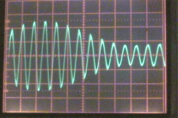
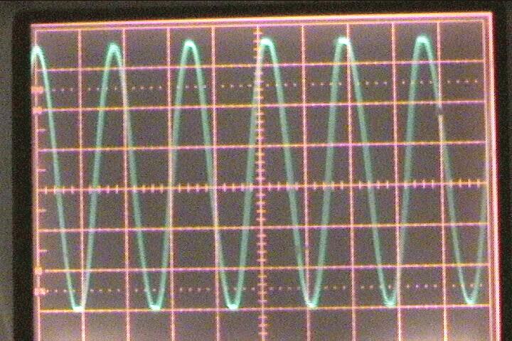
Photo 35: Scope waveform for RF Pre-Amp at T3 secondary -- Here's a view of the 7MHz signal as seen on the oscilloscope with the scope probe at the right side of R11/C15. By viewing the signal here and carefully turning trimmer cap C20 for maximum signal, you'll have half of the board's tuning complete! Scope settings: .5V/div, .2us/div yielding an approximate 1-2Vpp signal. My RF probe showed 0.938V. (Note that significant "hum" is caused by this test jumper, but it's a sufficient signal with which we can adjust the front end.)
Photo 36: Scope waveform at T2 primary -- This scope view is on the bottom (non V+) side of the T2 primary. Scope settings: 2V/div, .2us/div yielding a 4-8Vpp signal (again with hum), showing the gain of Q3. My RF probe showed 17V, but readings are somewhat suspect and arbitrary because of the hum. Individual mileage may vary.
Photo 37: Scope waveform at T2 secondary -- This scope view is taken with the probe on pad 3 of the (unpopulated) mixer IC U3. By viewing the signal here, you can peak the signal by turning the core of the T2 IF can. Scope settings: .2V/div, .2us/div yielding about a 1Vpp signal. My RF probe showed 0.4V. "Look ma, no hum!" But also note that this signal is unterminated and will change when U3 is soldered into the circuit.
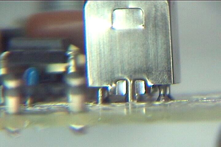
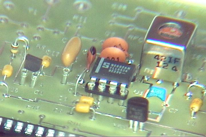
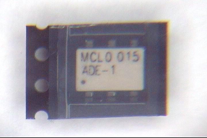
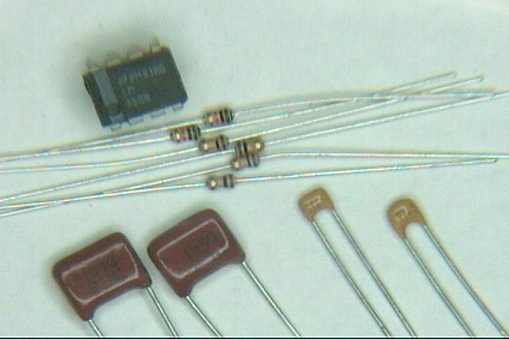
Photo 38: Mixer IC "U3" -- Shown inside its protective packaging
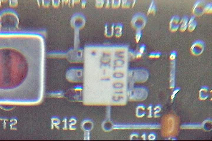
Photo 39: U3 out in the open -- It's tough to see, but mounting this little "surface mount" IC isn't as hard as people envision, mainly because the 0.1" lead spacing is the same as standard through hole DIP chips we're used to dealing with.
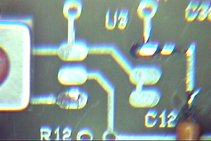
Photo 40: U3 pad #6 tinned and ready for the IC -- It's tough to see this shot, but tinning pad #6 allows you to place the chip in place and carefully, simply solder one lead in order to secure it to the board.
Photo 41: U3 in place, properly positioned over all pads -- It's important to ensure that all leads are positioned precisely over their respective pads. Then, the remaining leads can be soldered to their pads.
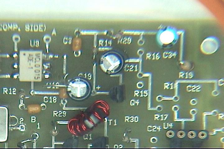
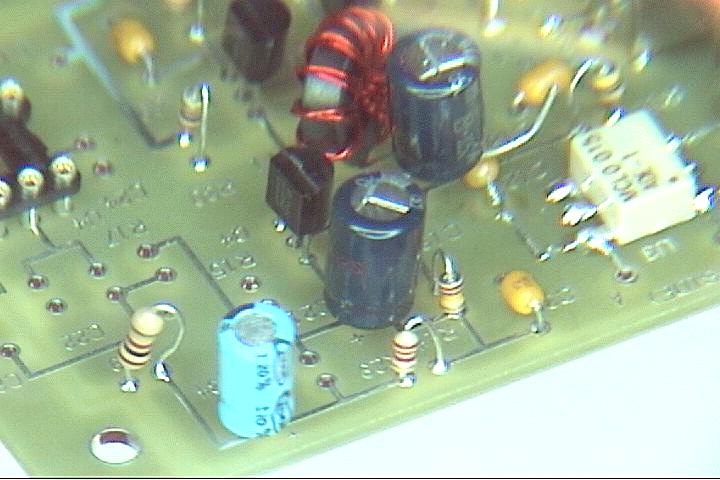
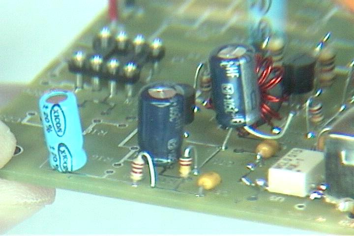
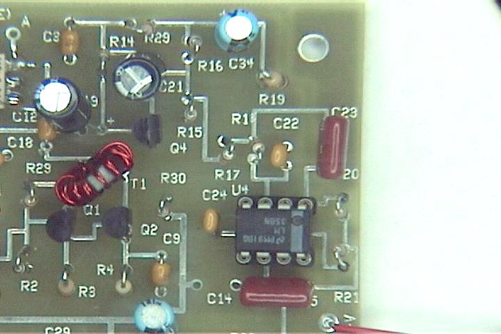
Photo 42: Components for the Audio Gain stage -- Shown are R12, C18, C19, R14, C36, Q4, C21, R31, C34 and R19.
Photo 43: Audio Gain stage complete -- All components for this stage are in place in this view of the board. Be careful of proper polarity for the electrolytic caps.
Photo 44: Side view Audio Gain stage -- This view shows the lifted negative lead for C19, in order to allow us a signal injection point when it comes time for test
Photo 45: The C19 "lifted leg" -- Another, clearer shot of the lifted negative leg of C19. (We'll tack this down onto the pad later, after testing is complete.)
Photo 46: Components for the Low Pass Filter -- Here you see U4, C22 and C24 (the smaller caps), C23 and C25 (the larger mylar caps), and resistors R15, R16, R17, R18, R20, and R21.
Photo 47: Low Pass Filter stage complete -- All parts in place.
Photo 48: Side view of Low Pass Filter -- Note that the leads for C23 and C25 mylar caps need to be compressed a bit in order that they fit into the space provided. Alternate parts were needed when it came time to "go production" with the board.
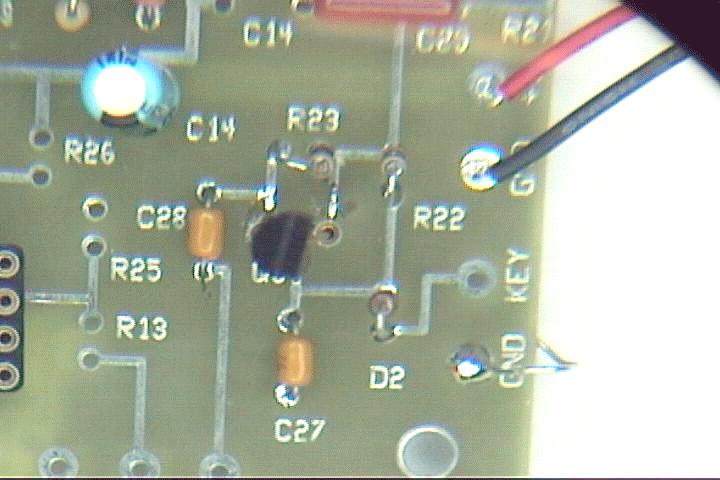
Photo 49: Components for the Muting stage -- Here you see Q5, R22, R23, D2, C28 and C27. Note the banded end of D2 being oriented at the banded end of the picture in the Layout diagram
Photo 50: Muting stage complete -- Note again the slight twist required to accommodate the lead-swapping of the FET transistor.
Photo 51: Side view Muting stage -- This view clearly shows the lead swapping, as showed in the diagram in the Parts Layout (dated 6/20/00 or later). Also note that I again used machined pin sockets for mounting these FET transistors, mainly because I wasn't 100% sure of the pinouts when I built this prototype board. (There were discrepancies in the datasheets that caused confusion for the layout of this part on the board.)
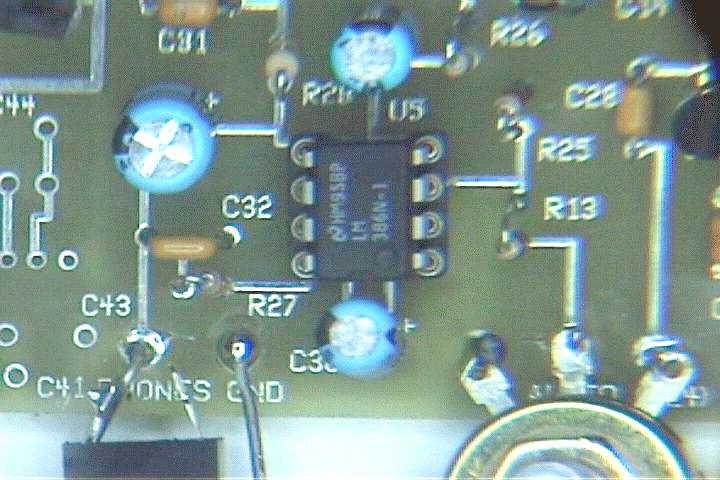
Photo 52: Components for the Audio Amp -- Shown are the 10K potentiometer (from the junk box or the Controls Option), C32, C33, C30, C29, C31, R27, R26, R13, R25, R28 and U5.
Photo 53: Audio Amp complete -- Again, note my special technique for temporary mounting of the external component R24 potentiometer. Also, be really careful with the polarity on all these electrolytic caps in the Audio Amp stage.
Photo 54: Components for the AFA Option
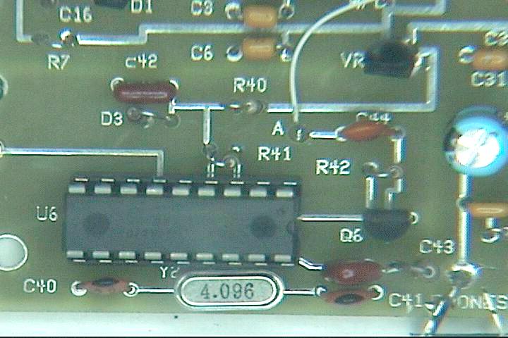
Photo 55: AFA Option installed -- Note jumper wire at pad A going over to the other pad A next to U3 (the U3 end is not shown here). This wire brings the LO signal over to the AFA circuit so its frequency can be determined.
Photo 56: Side view AFA components on the board -- Note one end of C43 being tipped up, as described in the Manual, to accommodate an extra 2-to-4 megohm resistor being placed in series with the cap. This is done to reduce the level of the AFA tone being injected to the LM386 amplifier. Also shown, but not too visible, is the 4.096 MHz crystal used for U6 being mounted slightly above the board. Mounting it flush on the board will short out some of the traces and not allow U6 to function properly.
Photo 57: Bypass Filter Mod for T2 -- One of the SOP builders found that front end RF sensitivity could be vastly improved in some cases by adding an R/C filter to the V+ supply to T2. A 47-ohm resistor is added in series with the V+ supply to the T2 primary by carefully slicing that pad on the bottom of the board and putting a 47-ohm resistor from it to the thin trace coming over to the transformer. Then, a .01uF capacitor is soldered from that T3 lead to the adjacent ground plane. (These two components, and clearer instructions have been provided to all first round customers.)
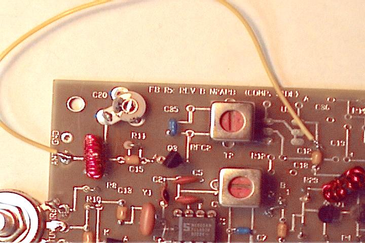
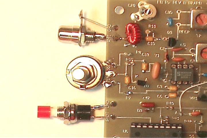
Photo 58: Completed PC Board -- Shown with all the external controls and jacks connected. This arrangement makes test connections on the bench a breeze!
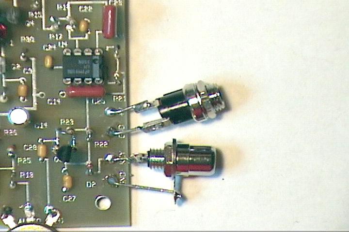
Photo 59: Close-up of the ANT, TUNE and SPOT external components
Photo 60: Close-up of the +V and KEYLINE connectors
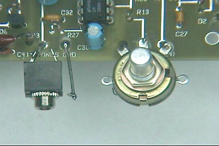
Photo 61: Close-up of the AUDIO LEVEL pot and the PHONES jack
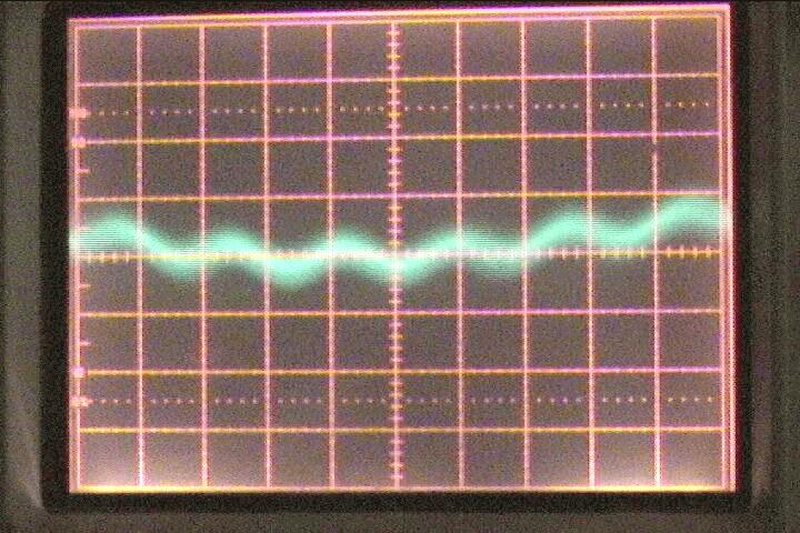
Photo 63: The audio test waveform -- Shown here is a very low level (approx 3mVpp), 550 Hertz signal that we inject into the start of the audio chain at the left side of C19. You can use the Twin-T Oscillator test circuit in the back of the manual, or as I used, a test oscillator on the workbench. By using a variable oscillator, I was ultimately able to find the peak frequency at which the Low Pass Filter was precisely passing, thus giving me the best response through the audio stages. You can use a potentiometer on the output of your test signal generator to provide the lowest possible signal to inject to the Audio Gain stage.
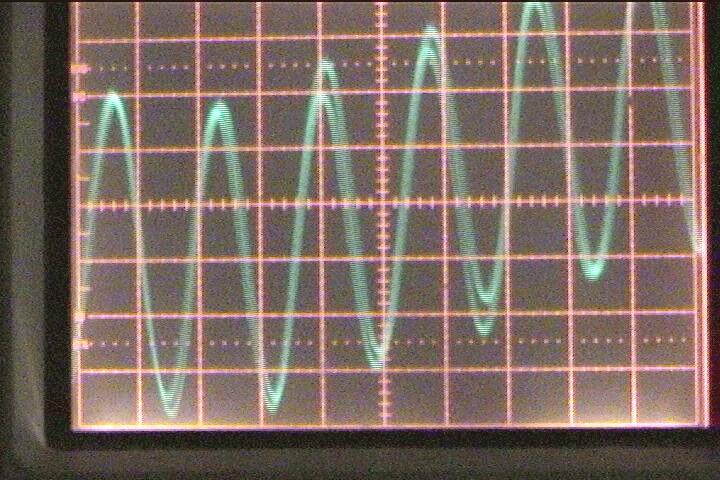
Photo 64: Scope waveform at Audio Gain stage -- The waveform here was obtained from the right side of C21. Scope settings: 50mV/div, yielding 250mVpp. My RF probe measured about 120 mV. Thus the gain of this stage is about 250/3 = ~80.
Photo 65: Scope waveform at middle of Low Pass Filter -- The waveform here was obtained from U4 pin 1. Scope setting: .1V/div yielding 550mVpp. Hence no gain here, per plan, just filtering.
Photo 67: Scope waveform at output of Low Pass Filter -- The waveform here was obtained from U4 pin 7. Scope setting: .2V/div, yielding 1Vpp. Simple gain of 2, plus (more importantly) filtering. My RF probe measured about .5Vdc.
Photo 68: Scope waveform at output of Audio Amp -- The AUDIO LEVEL control was increased to the point of just starting to see clipping at the top of the waveform (about 3/4 of the R24 potentiometer rotation). Scope setting: 2V/div, yielding about 13Vpp. My RF probe read about 6.7Vdc.
![]()
![]()
![]()