Full-color, full-resolution graphics from the pages of QRP Homebrewer
QHB #8 -- April 2002
|
Building the SOP Receiver ... Manhattan Style!, by Mike Korejwo, KB3HMR |
|
|
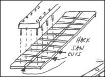
One way of mounting IC sockets "Manhattan-style"
|
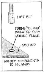
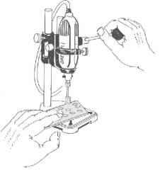
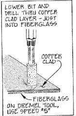
FIGURE 1:
Recalling the techniques used in drilling isolated pads with the
Islander Pad Cutter
|
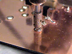
FIGURE 2: Close-up photo of Islander Pad Cutter and newly-cut island.
|
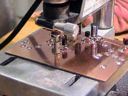
FIGURE 3: Photo of partially assembled base board in the drill press as I add a forgotten circuit node.
|
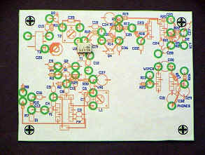
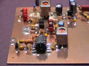
FIGURE 4: Photo of the template glued to the base board prior to drilling of the pads. Note the mixer chip (ADE-1) laying on the surface in its designated location to ensure proper pad location for its leads.
|
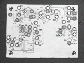
FIGURE 5: All the pads are cut now but the template hasnt yet been removed.
|
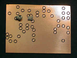
FIGURE 6: The template has been removed by soaking the board in warm water. The board has been cleaned, and the mixer chip and trimmer capacitor are set onto the surface to ensure good positioning of their pads.
|
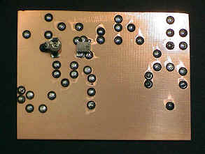
FIGURE 7: Each of the pads have been tinned by carefully heating them with an iron and applying solder. This will assure easier component attachment next. Note that the mixer chip and trimmer capacitor are now soldered in place.
|
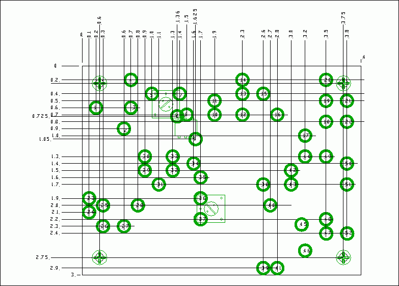
(Click image to view full-res) FIGURE 8: Base board pad locations. All dimensions shown in inches, referenced to top left corner (0,0). Note the four holes marked in the corners to facilitate ultimate board mounting to an enclosure, or perhaps for the attachment of rubber feet and standoffs.
|
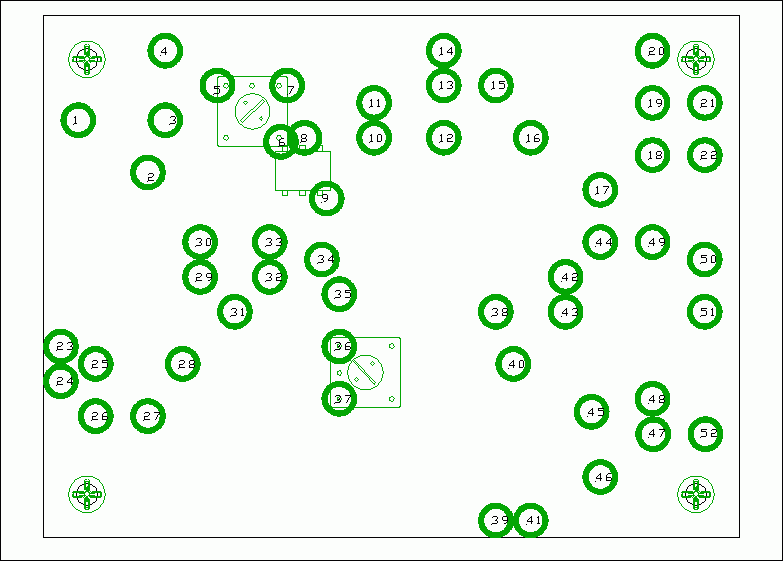
(Click image to view hi-res) FIGURE 9: Base board layout template (shown actual size). The numbers in each pad represent the circuit nodes to assist in attaching and connecting the components. Cut out this template and glue to the base board before drilling.
|
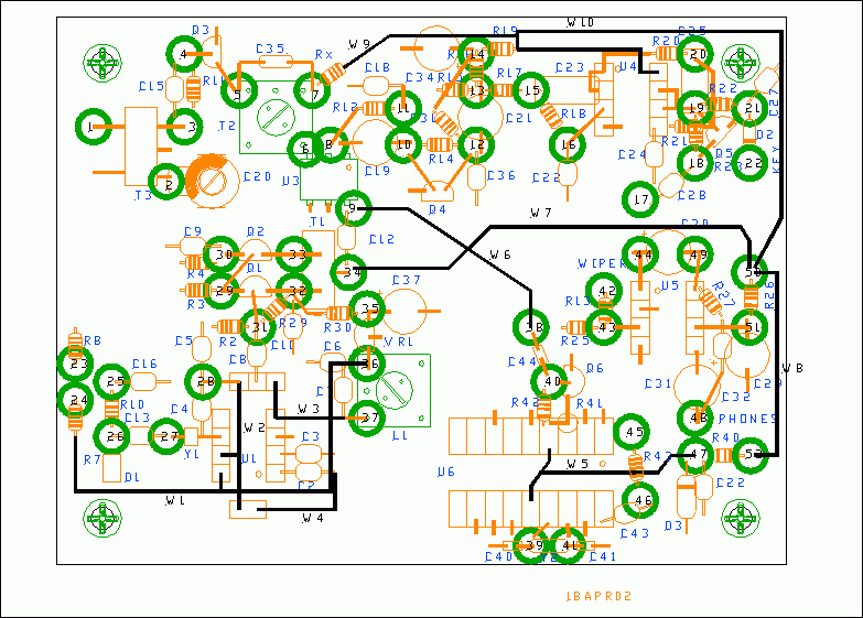
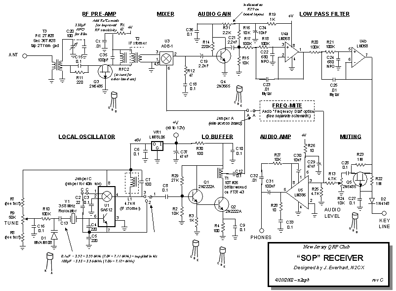
(Click image to view hi-res) FIGURE 10: Assembly diagram shows component placement and extra jumper wires needed to interconnect the functional modules. Use this diagram as the maser guide in attaching all components.
|
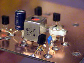
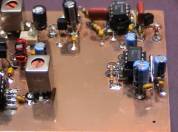
FIGURE 11: Close-up photo of IF transformer T2 and trimmer capacitor C20. Note the clean connections to the island pads.
|
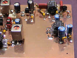
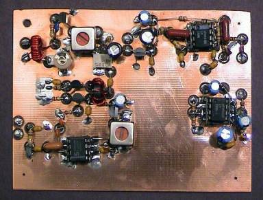
FIGURE 12: Photo of the right side of the circuit board with components and modules layed out as depicted in the schematic. (CW from bottom left): LO buffer, mixer, audio gain, low pass filter, muting, and audio amp. Note how the similarity to the schematic layout greatly assists initial construction and the inevitable debug to get it all working.
|
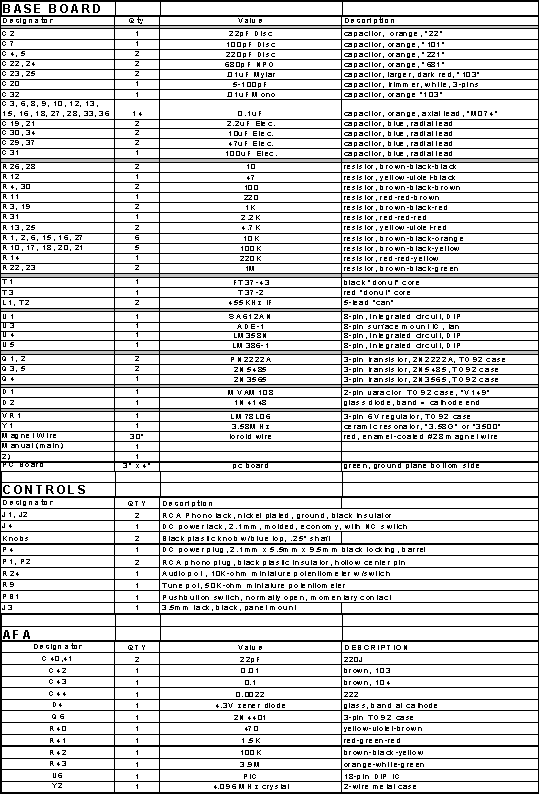
FIGURE 13: Parts List (Click image to view XLS file)
|
(Click image to view full-res PowerPoint file) |
![]()
![]()
![]()