NJQRP DDS Daughtercard
BUILDERS' NOTES
![]()
NJQRP DDS Daughtercard
BUILDERS' NOTES
![]()
Here are some important suggestions for assembling and using your DDS Daughtercard Kit.
Several notes are important at this point ...
(1) The SETFREQ program currently only works on computers running Win95 and Win98. We are working on adapting the program for use on other Windows operating systems (NT, ME, 2000, XP), and we'll let everyone know when this is available for download.
(2) Some homebrewers have noted that they get an error message "Could not open the DriverLINX driver" when trying to run SETFREQ. This can happen for several reasons, and can be easily remedied as described below ...
If you are successfully using SETFREQ, or (especially) if you are still having problems, Doug KA2UPW says to definitely contact him for some assistance. You can contact him at Dquagliana@aol.com .
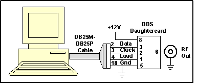
2) Schematic typos -- P1-1 and P1-2 schematic designators are reversed. The actual signals on P1 are correct (i.e., Load is on pin 1), so just change the schematic: P1-1 to P1-2, and P1-2 to P1-1. The latest online schematic and manual (version 1.3) have this correction.
3) MAR-1A amp device running
hot -- With the help of good
friends Jim Kortge K8IQY, Bob Johansen WB2SRF and Craig Johnson AA0ZZ, I was
able to get to the root cause of the amplifier running too hot on the DDS
Daughtercards. Turns out that bias and gain components were selected
based on the MAR-1 device spec sheet (which I had ordered/used in the
prototype builds), but Mini-Circuits sent me the new+improved MAR-1A devices
for the production run of parts. Thus a "mixed up spec sheet"
condition reigned and component selection for R1 and R4 cause the amps run too
hot in the first round of kits that were shipped.
Two different value resistors must be used for safe
operation. All those who purchased the first round of DDS Daughtercards
(i.e., shipped prior to August 29) have received a letter from the
NJQRP containing substitute resistors for R1 and R4, along with an
explanation of where these resistors are on the pc board and how they can be
easily installed in place of those initially shipped with the kit.
Actually, three different values of R4 were supplied to allow the user to
select the right one for each of three common supply voltages used by QRPers:
9V, 12V and 13.8V.
Once the corrected values of R1 and R4 are implemented, the
Daughtercard will typically produce an output of about 1V p-p from 10 kHz to
about 30 MHz. This corresponds to 2.5 mW output power, or +4 dBm. This
output level is consistent with the gain characteristics of the MAR-1A device
and the Daughtercard operates perfectly while becoming only mildly warm, as it
should.
4) Capacitor C8 ... This filter cap is not overly necessary, and depending on the specific bias level used for your MAR-1A amplifier, not including C* may further improve the spectral purity of the daughtercard's output signal. C8 is no longer provided in kits shipped from August 29 onward.
5) Soldering the DDS chip (U1) to the PCB If you attempt to solder the DDS integrated circuit onto the pc board yourself (i.e., instead of having someone else do it for you, such as KitBuilders), here is a slightly clearer method than described in the Manual ... Pre-solder pad for U1 pin 1, then carefully position the leads of U1 over its set of pads on the pc board. Re-heat the solder of pad 1 to reflow the solder onto U1 pin 1. This should leave the IC attached by pin 1. Again making sure the IC pins are aligned over all pads, carefully solder the opposite corner lead (pin 15) to its pad. This should leave all other pins of the IC aligned over their respective pads, making it easier to solder them to the pads. Go ahead and solder each of the other pins to their respective pads, being careful not to bridge across any adjacent pads. If this does happen, grab some solder wick or a solder sucker and use it to draw off the excess solder, which should be fairly easy and clean because of the solder mask on the circuit board.
6) Use of the DDS Daughtercard with the QuickieLab -- If you intend on using the DDS Daughtercard with the NJQRP QuickieLab, you must cut the +5V trace on the bottom of the QuickieLab pc board that leads to P1 pin 4 on the DDS Daughtercard socket. This is because the DDS Daughtercard produces its own internal 5-V supply and doesnt require that the QuickieLab supply it.
7) "Can I use the output of the DDS 'card to serve directly as a VFO for a transceiver?" -- If you have bias resistor R4 selected just right for the supply voltage being used, the signal purity of the DDS Daughtercard output signal should be more than sufficient to serve directly as the VFO for a transceiver. I use mine this way when operating my Wilderness Sierra. You can (and should) use an oscilloscope to check the quality of the output waveform, just to be sure, as I've found that different supply voltages from the one used to select the bias resistor can affect the output waveform symmetry and purity.
![]()
![]()